

In late 2025, something genuinely historic happened in the semiconductor world. It wasn’t a flashy product launch or a consumer gadget reveal. It was quieter, more technical — but far more important.
TSMC officially commenced volume production of its 2-nanometre (N2) process in Q4 2025, exactly as planned.
That single sentence carries enormous weight.
This milestone marks the beginning of the gate-all-around (GAA) nanosheet era for the world’s most advanced chips. It is the most meaningful shift in transistor architecture since FinFET replaced planar transistors over a decade ago — and it fundamentally reshapes what’s possible in performance, power efficiency, density, and system-level design.
This article breaks down what TSMC’s 2nm node really means, why it matters far beyond phones and laptops, and how businesses that understand this shift early can gain an advantage in AI, fintech, trading systems, and high-performance computing.
From FinFET to Gate-All-Around: Why N2 Is a True Architectural Shift
For years, semiconductor progress looked incremental on the surface. Smaller numbers. Slightly faster clocks. Marginal power savings.
Underneath, however, the physics was becoming brutally hard.
FinFET transistors — the backbone of 7nm, 5nm, and 3nm — were approaching their limits. As transistors shrank, leakage, variability, and power density became increasingly difficult to control.
Enter GAA Nanosheet Transistors
TSMC’s N2 node is its first production process using gate-all-around nanosheet transistors.
Instead of wrapping a gate around three sides of a “fin,” GAA wraps the gate entirely around stacked nanosheets of silicon. This gives engineers:
- Far tighter electrostatic control
- Reduced leakage at low voltages
- Greater design flexibility (tuning sheet width per use case)
- Improved performance at lower power
This isn’t marketing hype. It’s a structural change to the transistor itself, not just a shrink.
What TSMC Is Delivering with N2 (In Real Numbers)
According to TSMC’s disclosures and early customer guidance, N2 delivers:
- Up to ~15% performance improvement at the same power compared to N3E
- Significant power reduction at the same performance
- Higher transistor density, enabling more logic in the same die area
These gains compound at scale. A 10–15% uplift at the transistor level translates into dramatic real-world improvements once deployed across billions of transistors in modern SoCs and accelerators.
And importantly — this is volume production, not lab samples.
Why Q4 2025 Volume Production Is a Massive Signal
In semiconductor terms, “volume production” means:
- Mature enough yields to ship at scale
- Predictable performance and reliability
- Confidence from customers placing real orders
TSMC hitting its N2 schedule on time reinforces its reputation as the most reliable advanced node foundry on Earth.
This matters because only a handful of companies can actually use 2nm silicon — and even fewer can design chips that extract real value from it.
Who Benefits First from 2nm?
While consumer headlines focus on phones, the real winners sit elsewhere.
1. AI and Machine Learning Accelerators
AI workloads are brutally power-hungry. Every watt saved becomes:
- Lower operating cost
- Higher rack density
- More performance per dollar
2nm enables denser compute with lower energy leakage, directly improving inference and training economics.
2. High-Frequency Trading and Quant Systems
In ultra-low-latency environments, even small gains matter.
Lower power means:
- Less heat
- Higher sustained clocks
- Better determinism
For firms operating at microsecond and nanosecond scales, N2 opens the door to faster, more predictable execution pipelines.
3. Fintech and Secure Compute
Advanced nodes allow:
- Stronger on-chip security
- Enclaves with lower overhead
- More cryptography without power blowouts
As payments, wallets, and digital identity systems grow more complex, silicon efficiency becomes a competitive edge.
The Economics of 2nm: Why It’s Not for Everyone
Here’s the reality: 2nm is expensive.
Mask costs, design complexity, and validation effort are enormous. This node isn’t about cheap chips — it’s about strategic chips.
That’s why we’ll see:
- Fewer but more powerful dies
- Chiplets and advanced packaging
- Purpose-built silicon rather than general compute
The winners won’t be those who merely adopt 2nm — but those who architect systems correctly around it.
Advanced Packaging: The Silent Partner to 2nm
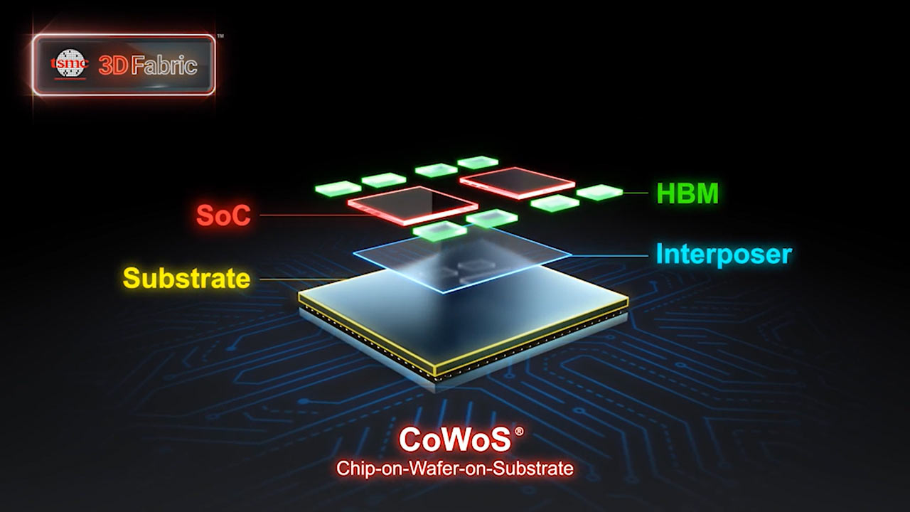
TSMC’s roadmap doesn’t stop at N2.
2nm is designed to pair with:
- Advanced 2.5D and 3D packaging
- Chiplet-based architectures
- High-bandwidth interconnects
This means:
- Mixing process nodes intelligently
- Separating logic, memory, and I/O
- Optimising cost while retaining performance
The future is not “one giant die” — it’s systems-on-package.
N2P, A16, and What Comes Next
TSMC has already outlined follow-on variants:
- N2P for higher performance
- A16 with backside power delivery
These enhancements further reduce resistance, improve power integrity, and push performance envelopes beyond what today’s systems can achieve.
By 2026 and beyond, we’ll see platforms that simply weren’t feasible on older nodes.
What This Means for Software, AI, and System Design
Hardware changes everything upstream.
With 2nm:
- AI models can grow without linear power growth
- Real-time analytics becomes cheaper
- Edge devices gain server-class capability
But only if software and architecture keep pace.
Throwing old code at new silicon wastes the advantage.
Why This Matters for Australian and Global Businesses
Australia punches above its weight in:
- Fintech
- Trading systems
- AI research
- Defence and security tech
But success depends on integration, not just adoption.
Understanding how new silicon impacts:
- Infrastructure
- Latency
- Cost models
- Security
…is what separates leaders from followers.
The Strategic Reality: Silicon Is Back at the Centre of Power
For years, software stole the spotlight.
Now, the pendulum is swinging back.
Advanced silicon determines:
- Who can run the biggest AI models
- Who processes payments cheapest
- Who trades fastest
- Who secures data best
2nm isn’t just “smaller chips”. It’s strategic leverage.
Where Digital One Agency Fits In
This is exactly where Digital One Agency operates.
We don’t just build apps or platforms — we design systems that align software, infrastructure, AI, and emerging hardware realities.
Our work spans:
- AI platforms and embedded intelligence
- Fintech, blockchain, and payment rails
- High-performance and low-latency systems
- Secure, scalable architectures built for the next decade
We help clients:
- Understand what technologies like 2nm actually enable
- Architect systems that benefit from them
- Avoid costly mistakes chasing hype without strategy
The Takeaway
TSMC’s move to 2nm volume production in Q4 2025 marks the start of a new era.
An era where:
- Efficiency matters more than brute force
- Architecture beats raw scale
- Those who plan early win
The question isn’t whether 2nm matters.
The question is whether your systems, software, and strategy are ready for what comes next.
Book a Free 1-Hour Strategy Session
If you’re building — or planning to build — platforms in AI, fintech, payments, or high-performance systems, now is the time to get ahead.
Let’s talk strategy, not buzzwords.
👉 Book a meeting: https://digitaloneagency.com.au/book-a-meeting/
📞 Call us globally 24/7: +61 2 9057 9079
📧 Email: contact@digitaloneagency.com.au
Digital One Agency — building what’s next, before it’s obvious.
Need Custom AI & RAG Pipelines in Australia or the UK?
Digital One Agency is a senior, founder-led engineering team based in Australia (Gold Coast HQ) with active UK clients in London, Manchester and Edinburgh. We build production RAG pipelines and bespoke AI systems — fine-tuning, vector search, evaluation harnesses included.
- Free 30-minute discovery call with a senior engineer
- Fixed-scope quote with milestone billing — no hourly rates
- AU & UK references on request
- Bespoke code you own — not a SaaS reseller, not a ChatGPT wrapper
Book your free discovery call → Or send us your project details


